MAKE A MEME
View Large Image
| View Original: | Gerber-layers-example.png (232x1000) | |||
| Download: | Original | Medium | Small | Thumb |
| Courtesy of: | commons.wikimedia.org | More Like This | ||
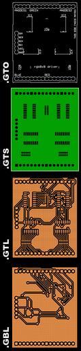
| Keywords: Gerber-layers-example.png Board design and Gerber file format image en wikipedia org/ Gerber-layers-example png 19 47 8 February 2009 en User Halley Public domain thumb left German version Board design and Gerber file format image created by Ed Halley custom for Wikipedia article Gerber File Example Gerber layers showing GTO file describes the top overlay silkscreening to document the parts GTS file describes the top solder resist a protective film to avoid stray solder GTL file describes the top layer copper traces the rest is etched away GBL file describes the bottom layer copper traces of a printed circuit board Not shown any silkscreening or solder resist on the bottom of the board and a definition of all drill sizes and locations Some designs may also have more copper layers sandwiched between boards Printed circuit board layout | ||||